True to its “mens et manus” motto, MIT is recognized worldwide for emphasizing integration of rigorous academics with practical engineering aimed at addressing some of society’s greatest challenges. Attracted by that reputation for fusing scientific theory with hands-on problem-solving, Hazzel Fernández recently spent a week at MIT participating in an immersive workshop in nanotechnology – part of a collaborative program with Mexico’s largest private university, Tecnológico de Monterrey (Tec).
“It’s really exciting to be here,” said Fernández, a biomedical engineering student at Tec’s Guadalajara campus. “In Mexico, it (MIT) is something you look up to. It goes beyond theory…it’s getting to do things instead of just understanding how they work and thinking about doing them.”
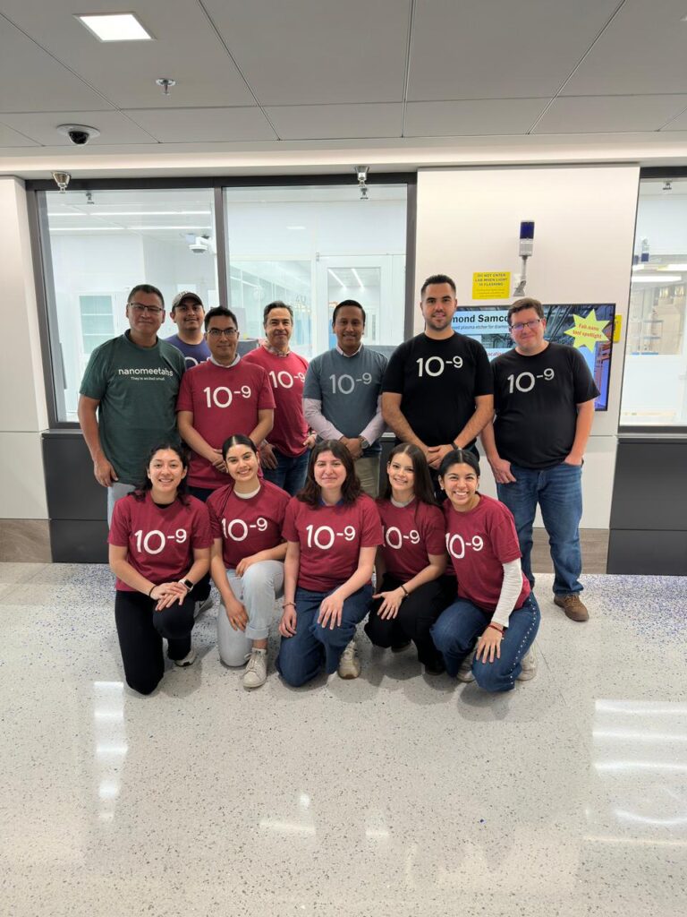
Fernández is one of ten Tec students and who took part in this month’s nanoLab workshop. Conducted six times annually, nanoLab is a key initiative of the MIT- Tecnológico de Monterrey Program in Nanoscience and Nanotechnology – a multidisciplinary collaboration between Tec and MIT launched in 2014.
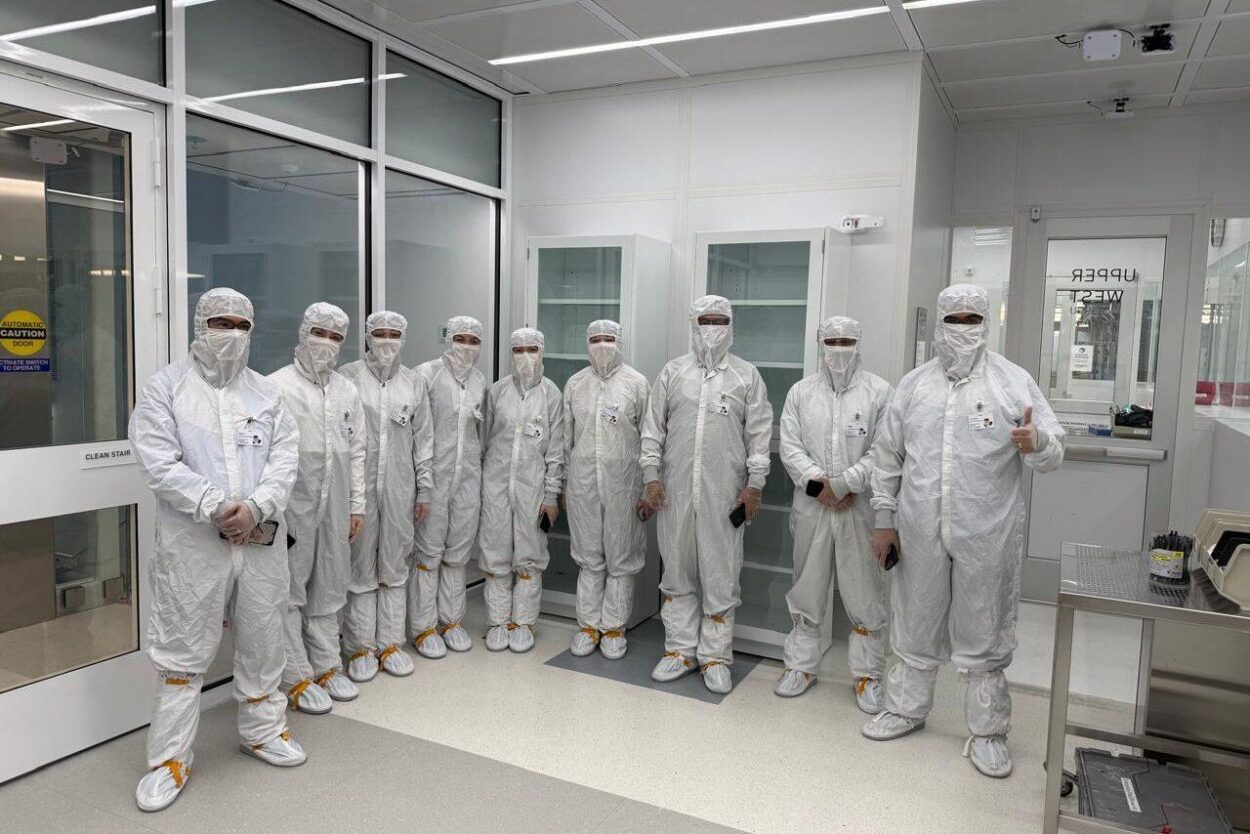
A September 2025 report on the collaboration notes that it is “widely recognized as a model for international academic partnerships,” training more than 40 Tec students during in-person workshops each year and having reached over 1,000 students through a virtual nanoLab education class. During the workshops, Tec students receive a hands-on introduction to nanofabrication at MIT.nano, MIT’s center for nanoscale discovery and innovation located in the Lisa T. Su Building. Workshop participants design and fabricate devices such as solar cells, while learning about data analysis, cleanroom techniques and fabrication flows.
During the week of May 4, Fernández and other students from Tec campuses across Mexico participated in approximately 30 hours of hands-on work fabricating and testing three devices designed to illustrate important microfabrication techniques:
- a solar cell as an example of an electronic device;
- a microcantilever as an example of a microelectromechanical system; and
- a microfluid device.
Students gained practical experience in various state-of-the-art nanofabrication techniques, including photolithography, etching, chemical and physical deposition methods and device characterization. In addition, they heard talks by MIT researchers on topics such as microelectronics, robotics, photonics and biosensors.
The weeklong nanoLab is among several components that comprise the MIT-Tec Program. The FrED Factory – a factory-like education platform that involves Tec undergraduates in manufacturing low-cost, desktop fiber-extrusion devices (FrEDs) – is another essential element of the program. According to the 2025 MIT-Tec Program annual report, the FrED Factory has been incorporated into multiple courses at Tec de Monterrey, “giving students practical experience in designing and refining smart manufacturing systems.”
The MIT-Tec Program also offers Tec students semester-long research experiences within MIT’s Department of Mechanical Engineering. Following the first cohort of seven Tec students in 2024, eight students traveled to MIT for the Undergraduate Research Stay during the 2025 Fall semester.
“The strength of the MIT- Tecnológico de Monterrey Program lies not in any single component but in how its elements reinforce one another,” said Vladimir Bulovic, Fariborz Maseeh Professor of Emerging Technology and Director of MIT.nano. “Early hands-on experiences like nanoLab connect naturally to opportunities such as the FrED Factory undergraduate stays and research residences, creating a continuous pathway from exposure to application. Together, they not only shape how students learn, but also deepen collaboration between the two institutions, strengthening a shared approach to innovation across borders.”
Each nanoLab cohort brings together undergraduate students—and occasionally graduate students, postdoctoral researchers, and faculty members—selected through a competitive process from more than 20 Tec de Monterrey campuses. The program gets approximately 200 applicants annually and admits about 60 each year, said Leonardo Farfán Cabrera, a Research Professor in the School of Engineering and Sciences at Tec’s Puebla campus.
“One of the most important takeaways has been learning how MIT.nano works. Labs in Mexico are run very differently,” said Farfán Cabrera, who attended the workshop in May. “Here at MIT, we’ve been spending hours in the clean room every day. We see how students and researchers do hands-on work outside the classroom. When I get back, I will work on reorganizing my lab based on what I’ve learned at MIT.nano.”
Over the course of one week, Farfán Cabrera said he’s learned how to make processes more efficient and how to reduce risks in the lab.
“This program, in only a few days, has changed my vision,” he said.
Andys Hernández Peña, a postdoctoral researcher at Tec’s Puebla campus, agreed that the recent week at MIT.nano was “transformational”.
“It has made me rethink what is possible. I will leave MIT with a new understanding of where technology is headed. My perspective has changed,” said Hernández Peña, adding that a key benefit of the nanoLab workshops is the strengthening of ties between MIT and Tec.
For Tec students, opportunities to interact with MIT researchers representing a range of academic disciplines is another valuable aspect of the nanoLab experience.
“The workshop offers a unique opportunity to network with experts and peers, enhancing their academic and professional development,” said Arnoldo Salazar Soto, an adjunct researcher in nanotechnology and semiconductors in the School of Engineering and Sciences at Tec’s Monterrey campus.
Reflecting on her week at MIT, Hazzel Fernández echoed those sentiments.
“This week at MIT.nano has been an eye-opening experience,” she said, adding her appreciation for being able to “learn and explore” with an array of MIT students and faculty. “I think that’s the best part of being here. Also being able to be around people who are super curious. People here are ready to develop all these new things and to discover.”